Saturday, April 24, 2021

PDP-11/70: Even More Stuff

January 2021: Debugging Commences

In my last post I left off my tale of PDP-11/70 restoration in late January, having just powered up the rebuilt supplies after reinstalling them in the chassis.  The next step was to reinstall the processor, cache, and memory and see what happens:

(not quite) The First Power-up with Stuff Installed

The answer is: not much.  The processor was almost entirely unresponsive: it powered up with the RUN and MASTER lights on and wasn't responding to most input from the front panel.  Toggling the "Halt" switch and hitting "Start" caused the RUN light to go out, but that's the only response I got from the console.

Enter the KM11-A:

How does one debug a processor as complex as the 11/70's?  These days, advanced diagnostic tools like Logic Analyzers and digital storage oscilloscopes are commonplace, but in 1974 they weren't really an option.  DEC's solution to this was the KM11-A "Maintenance Set", a pair of boards with an array of lights and four switches.  The lights were used to monitor device state, and the switches controlled the behavior of the device and allowed for single-stepping processors.  The KM11 could be used to debug a variety of DEC hardware -- various PDP-11 processors and a few different peripherals and device controllers.  My KM11-A is a reproduction, which I built over a decade ago to debug my PDP-11/40, since then I've also used it to repair my PDP-11/05.  And now, it's time for the KM11 to work its magic again.

With the KM11 boardset installed  (you can see it sticking out from the left-hand side in the above picture) I was able to step the processor through micro-instruction execution.  A toggle switch on the KM11 clocks the processor, and the DATA lights on the front panel show the microcode address in the right 8 bits (with the selector knob turned to "uADDRS FPP/CPU).  (In the above picture it's showing address 200 octal).  The PDP-11/70's KB11-C processor is microcoded, using an array of small, high-speed bipolar PROMs to store 256 64-bit microcode words.  These 256 words are interpreted by the hardware to implement the PDP-11 instruction set, address memory and the Unibus, and to interface the processor to the front panel.
 
The KB11-C Engineering Drawings contain 14 pages of "flow diagrams" which detail precisely how the microcode executes.  The "KB11-C Processor Manual" (EK-KB11C-TM-001) provides 376 pages explaining exactly how the hardware works.  A typical flow diagram looks like:
Feel Flows
This is FLOWS 14, which diagrams the Console (front panel) portion of the microcode.  Top-center, you can see a starting bubble labeled "CON.00" which marks the start of the console portion of the microcode.  The box below it represents a single microinstruction, and details the operation of this microinstruction in each of the processor instruction cycle's "T-states."  The arrows coming out of this box indicate branches to other microinstructions, depending on the state of the hardware at the time of the instruction execution.  Branches may also lead to other flows (indicated by diamonds). 

Use of the KM11 indicated that the processor was definitely executing microinstructions, and seemed to be following the flow diagrams in the engineering drawings.  This is excellent -- it indicates that a lot of the hardware is functional.
 
Curiously, left to its own devices the processor didn't seem to be executing microinstructions at all and was stuck at micro-address 200 octal.  This is "ZAP.00" in the flow diagrams and is where the processor starts at power up or after a reset.

In the troubleshooting section of the 11/70 service docs (diagram on p. 5-16) it states:
IF LOAD ADRS DOES NOT WORK AND:
- RUN, MASTER & ALL DATA INDICATORS ARE ON
- uADRS = 200 (ZAP)
THEN MEMORY HAS LOST POWER
Which seems to adequately describe the symptoms I was seeing -- there is power-fail hardware in the processor that forces the microcode address to 200 in the event that power is lost, but the AC and DC LO signals (which are what the power supply uses to tell the processor of such a failure) were all fine (after checking again, just to be sure).   Also if this was the case I wouldn't expect that the KM11 would be able to step the processor at all -- the power fail hardware should force the processor's microcode address to 200 at all times until the power failure is resolved.

Probing the processor clock signal on the backplane with an oscilloscope revealed no clock signal at all, just a flat line.  The clock signal is provided from one of three sources on the "TIG" (Timing Generator) board:  Normally it comes from a 33.3333Mhz clock crystal.  While debugging with the KM11, it can come either from the MAINT STPR switch on the KM11, or from a special diagnostic RC clock network on the TIG board (this latter can be adjusted to a wide range of frequencies for margin testing.)  This lack of a clock signal was definitely an important clue.

Another oddity was revealed after a closer look at the service docs: In Chapter 4 of the Processor Manual, Section 4.1.3 it states:

"The third source of timing [the other two being the crystal clock and a diagnostic R/C network] is the manually-operated, single-step MAINT STPR switch S4, located on the maintenance card.  This switch is only enabled when maintenance card switches S2 and S3 are both set to 1."

Section 4.2.3 confirms this:

"The maintenance card S2 and S1 switches are both set to 1 to allow single timing pulses to be generated by MAINT STPR switch S4.... Removing the S2 or S1 input conditions the MS EN flip-flop to be cleared."

What was interesting about the above is that on my system, switch S4 (MAINT STPR) stepped the processor with switches S1 and S2 set to any configuration.  This being the case, I wondered if the logic that selects the clock source was faulty, and was always selecting the MAINT STPR input.
 
Well, only one way to be sure, and this would require getting the TIG board out on an extender for some extensive probing.  In doing so, I found that no clock signal was being generated by the 33.3333Mhz crystal at all; in fact while probing it one of the legs to the crystal fell right off.  This is usually a sign of a faulty component.

So I placed an order on Digi-Key for a replacement.

But then I got impatient and remembered that the rusty burned-out hulk of a PDP-11/45 I picked up along with the 11/70 was in the garage, and the 11/45 also has a TIG board, very similar to the one in the 11/70, and also using a 33.3333Mhz crystal.  
 
A short while later, the 11/70s TIG had a new, stolen, clock crystal:
Where'd you get that shiny new crystal?

And after reinstalling the TIG back in the backplane and powering up:


It's alive!  A bit.  With a working clock, the processor was able to respond to the front panel and I was able to load addresses and examine and deposit into memory.  However, instructions would not execute -- loading an address and hitting "Start" on the front panel had no effect.  More pressing: after the system warmed up for a minute or two, the "Load Address" switch on the front panel would stop working properly, and would always load "0" rather than what was in the front panel switches.
 
Still, good progress for just a few evenings of research and debugging (and conversing with people on cctalk for advice.)  Over the next few days I started in on investigating these issues... which I'll talk about in my next exciting installment.  Until then... go find something else to read.


Saturday, April 17, 2021

PDP-11/70 Repair: Part One

Looks like a few months have passed since my last post, as seems to be typical.

Never you mind, let's just ask the question: How'd that whole "Restore a rusty soot-covered PDP-11/70" thing turn out?  Well, I don't want to spoil anything.  Let's pick up where we left off.


November 2020:Make it Look Good

Looking good!

Well, first I installed the replacement front panel assembly.  That'll get you 90% of the way there, as anyone who restores old computers can tell you.

December 2020, January 2021: Cleaning, Capacitor Reforming, and Fan Replacement

Despite a pretty new face, the computer was still extremely dirty.  When I first brought the system home I'd given the rusty parts a rough sanding to get rid of the grit and loose paint, but the inside of the chassis was still amazingly filthy. 

Dirty Little Fingers

The boards themselves cleaned up quite well: they were all covered in a fine grit of soot and who knows what else, but soaking them in warm soapy water for 10-15 minutes then scrubbing with an old toothbrush eliminated most of the detritus.  After drying in front of a box fan, the gold fingers were cleaned up with liberal use of Scotch Brite(tm) cleaning pads.  

None of the 17 boards that comprise the Processor, Cache, and Memory of the system appeared to be seriously damaged.  That's good!


My next major concern was whether the backplane itself was hiding some corrosion -- corroded pins make poor contact with the boards and might never work reliably.  And these pins aren't exactly trivial to replace -- while it might theoretically be possible to undo the wire wrap to a bad pin, desolder it from the backplane assembly PCB and remove it... no, you know what: it's impossible for all intents and purposes.  If you have a dead pin on a backplane like this, the backplane (and it follows, the computer) is toast.

This weighed fairly heavily on my mind, as soot and moisture could easily have destroyed this computer.


Empty backplane, mostly.
With the boards removed for cleaning the chassis was now empty, with the backplane exposed for easy (if extremely slow and somewhat painful) cleaning. There are 44 slots in the KB11-C backplane, each of which is divided into 6 sections, designated A-F.  Each one of these sections needed to be cleaned.  A strategy I've used in the past is to fold a thin piece of cardboard over a credit card; this jerry-rigged assembly can be dipped in 99% isopropyl alcohol and then used to clean the slot by inserting it and removing it a few times.  Accumulated dirt and light corrosion will be pulled off leaving the slot at least slightly cleaner than it started off.  For good measure, before starting on each slot, I gave it a good dose of contact cleaner to help loosen things up.

Repeat this for all 6 sections of all 44 slots.  I did this over the course of about three weeks, a few slots every night to prevent my fingers from falling off.  Most of the slots were already pretty clean, but on a few the cleaning card came out quite dirty and required a few extra passes.  The last few slots toward the rear of the chassis took the most time to clean.

Had I to do this again, I might have tried removing the entire backplane from the chassis and rinsing it out with water or isopropyl first, but I got pretty good results with this approach.

Reforming Capacitors

In the midst of the above cleaning process, I started in on the power supplies.

The PDP-11/70 gets its power from two H7420a power supplies.  Each H7420 is a large bulky unit with an extremely heavy transformer up front; this transformer provides 30VAC to up to five modular power supply units which take the AC and provide regulated DC.  Different modules provide different voltages; the H745, for example, provides -15V at 10A; the H744 provides +5V at 25A, the 754 gives you +20V and -5V.

Depending on what system you have and what options it has fitted, the H7420 might have a variety of these modules installed.  For the PDP-11/70 system I have, it's entirely H744s -- seven of them, providing a whole lot of +5.  The H7420 itself provides + or -15VDC, as well as 8V and the ACLO and DCLO signals used to let the computer know if it's about to lose power.

A really dirty H744, prior to cleaning.

Over the course of a month, each of the H744s was removed, disassembled and cleaned.  The capacitors were removed and reformed.  Normally, I like to replace capacitors, rather than reforming just for the sake of reliability and peace of mind.  However, I thought I'd give reforming a try this time around, mostly due to cost considerations:  Each H744 contains three large capacitors, and with seven of them to restore (plus two extra for spares that I happened to have lying about), it was looking like I'd be investing about $750 to replace them all.

I won't go into details on capacitor reforming here -- it's well documented all over on the 'net (David Gesswein has a nice write-up here) and it's not all that exciting.  The upshot of my reforming experience was that of the 28 capacitors in the supplies, four of them ended up being marginal, and two were completely dead.  Not too shabby.  

Testing of the supplies (and the capacitors) was done using an electronic load that I bought for the occasion.  It's a lot more convenient than using banks of resistors, and it looks cool too:

Burning in an H744 (middle) on the bench.  Electronic load on the left, H7420 on right.

The electronic load gives me the ability to vary the load while testing, starting with a small amount of load for initial smoke testing, then ramping it up to really soak test the thing.  I let them run for a couple of hours each.  While this is going on, the output of the supply is monitored on an oscilloscope, to check that ripple is within tolerances (about 200mV, max). This is also a good time to do an initial adjustment of the voltage level (each H744 has a small potentiometer exposed on the front that is used for this purpose).

Of the 9 H744s, all but one tested out fine and required no additional repairs.  The one that failed would occasionally make an interesting short squeaking noise, with an associated drop in voltage.  I put that one back on the shelf for a future investigation (which as of this time has not yet occurred).

Fan Replacement

I have neglected to mention the state of the fans in this system: they were bad.  Very bad.  There are 18 fans in the PDP-11/70: 8 in the two H7420s, and 10 in the processor chassis.  Of these 18 fans, only three actually spun freely and even those sounded pretty bad when doing so.

OBEY THE PAPST FAN

I opted to replace these entirely.  While some of them were designed to be disassembled and cleaned, they were all rusty to the point where I just did not want to bother.  I found a decent supply of Papst fans on eBay for a reasonable price.  These are nice fans, well built with metal blades rather than the more common plastic ones.  Heavy.  Elegant.  Subtle.  Hungarian.  I like them.  

I installed 8 of them in the H7420s and reinstalled six of the H744s (and one H7441 that snuck in there while I wasn't looking.  See if you can find it, it's really exciting).

The supplies: all cleaned up and put back together!

At this point, all the wiring was double-checked, both for continuity and also for shorts and breaks in the insulation.  Everything checked out OK, so I fired the system up with an empty processor chassis, while holding my breath:

Hey, not bad.  No smoke or fire or bad smells, and the front panel lit up (all the lights are on by default since it's disconnected from the logic that normally drives it).  All voltages at the backplane were tested, per the service manual:

This is actually kind of a pain in the neck because you're finding tiny pins in a rat's nest of


The wire-wrap side of the 11/70 backplane: Where's Waldo?

and trying not to accidently brush against another pin while doing so.  I used a set of small jumper wires that clip over the ends of the wire-wrap pins to help keep things isolated.  Even so it was kind of nerve-wracking.  Long story short: all voltages were present in the right places on the backplane, and the ACLO and DCLO signals were both high, as they should be.

Conclusion:

As January drew to a close, I had gotten the PDP-11/70 to a point where it was clean and safely powering up.  What would the following months bring?  STAY TUNED TO FIND OUT!


Saturday, December 5, 2020

A Small Detour: PDP-11 Rescue!

(I do have some new MDP-1000 information, I do, really.  There's even some at the end of this post.  So read on!)

Sometimes you gotta do something stupid for your hobby.  Like, really, really stupid.  This is one of those times. Back in October, a post appeared on the Vintage Computer Forums:


In case it's not clear from the text, a collector in Silicon Valley was looking to part with a pile of PDP-11 systems that had been in a fire many years ago.  Here's a couple of larger pictures:


What we have here are two of the more interesting (and desirable) blinkenlights PDP-11 systems:  A PDP-11/70 and a PDP-11/45.  Unfortunately, neither of them looked to be in particularly great condition -- the 11/45 in particular looked like it spent some time in a blast furnace.  My first thought was that these systems were a lost cause.

But.

But but but.

The 11/70 is on my short list of "Computers I Just Gotta Have" but they're rare enough, and sought out enough in the collector community that finding one for a price I can afford seems almost an impossibility.  (The 11/45 is a really nice computer, too.)

Hmm.

Despite their condition, I was intrigued, and so I reached out to the seller who informed me that I was the only one who'd contacted him, which I still find very surprising.  I don't live in California but I have a friend who lives near the seller, and he kindly offered to go out and take some more detailed pictures so I could more accurately assess the condition of the systems.  

And wouldn't you know it, things didn't look so bad on the inside:  Here's a few shots of the innards of the 11/70:


Filthy, yes.  Melted?  Not so much.  Except for those fans at the top there, where the plastic fan blades kind of became liquid and dripped down on everything below them.

Melty!

Apart from the melted front panel and fans, the thing looked totally fine.  Backplane clean, wirewrap undamaged, power supplies present, CPU board set complete.  And more interestingly, take a closer look at the cards in the card cage in that first picture there.  Those of you keen of eye and well-versed in PDP-11/70 lore might notice the "Setasi" label on the boards on the left-hand side.  That's an aftermarket boardset -- the Setasi Hypercache + PEP70, which replaces the original memory and cache of the PDP-11/70 system.  It gives the system a full 4MB of memory, and that memory runs at the speed of the 11/70's cache.  It's a rare upgrade, and aside from making the system faster, it's really useful:  normally the 11/70's memory resided in an external rack and took up multiple cabinets with their own large power supplies.  The PEP70 provides an entire 4MB of memory on a single board!  Here's another view of those boards:

Oh yeah.  That's the stuff right there.

Well, that's tantalizing, for sure.  But what about the 11/45?


It's a bit more rough.  In that top picture you can see that in addition to the front panel being melted away, the power distribution wiring harness is completely toast.  And there's not much paint left on the thing and rust has taken its place.  But again, the boards are all there and look to be in decent nick (apart from a slightly melted handle on that M9301 Bootstrap Terminator there in front).  And miraculously the backplane looks to be completely unharmed, apart from some charred detritus stuck in the wirewrap pins.  It seems like the metal of the chassis and the power supplies shielded the processor from the brunt of the heat.

Needless to say I decided to take the plunge.  I had already been planning a trip to the bay area to pick up some other items and to help out a friend with a Xerox Alto restoration, why not add a couple of rusty racks worth of slightly melted PDP-11 gear to the haul?  I struck a deal with the seller, and the first weekend in November I rented a cargo van and drove 14 hours from Seattle, WA to Cambpell, CA.  

All told, that weekend I picked up the two PDP-11s, a Three Rivers PERQ 1A workstation, two General Automation SPC-12 minicomputers, a Symbolics 3620 workstation, a pile of Symbolics and TI Explorer documentation and parts, and two Unibus memory cabinets that might have been a part of C.mmp at one point.

Oh, and a replacement front panel for the 11/70, kindly sold to me at a very reasonable price by a good friend of mine:

Is there anything more beautiful?

Then I got in the van and drove back.

Over the past couple of weeks I've been slowly going over the two PDP-11 systems, preparing a plan to tackle their restorations.  I've decided to start with the 11/70 since it's the cleaner (and more exciting) of the two systems.  The rack has been lightly sanded down and cleaned, so it's no longer covered in a gritty layer of rust and soot and melted plastic, and the same process has been started for the processor chassis.  Once spring rolls around I plan to repaint the rack and the chassis, but for now I just want them clean enough so that my hands don't get filthy when I work on them.

The next step is to clean the backplane and the boards and then tackle restoring and testing the power supplies.  I've ordered a ton of isopropyl alcohol for cleaning the backplane slots, and once it arrives the cleaning can commence.

What about the MDP-1000, huh?

Sure, sure.  Recall that I mentioned picking up a couple of SPC-12s in my California haul?  Well, here they are!


As I mentioned in my last post, the MDP-1000 is a rebadged/repackaged SPC-12.  Now I have the original to hack on as well!  And I have some documentation for these!  More information in my next post, I swear!

Until next time!


Monday, October 19, 2020

The Motorola MDP-1000

So having found myself gainfully employed again after a rather stressful hiatus over the summer, I decided to reward myself and splurge on this sexy bit of kit:

The Motorola MDP-1000 Minicomputer

Prior to this showing up on eBay, I wasn't even aware that Motorola had ever made a minicomputer (more on that later), but there it was.  I knew I had to have it.  It arrived last week and I've been digging into the system and trying to find out more about its history.  Unfortunately not much is out there, so I thought that it would be a perfect subject to write about here so that the majesty of the MDP-1000 might be more widely shared with the world.  Also, what else am I going to do with myself late on a Sunday evening?

The Hardware

The MDP-1000 was introduced in late 1968 or early 1969 and is built from discrete TTL and DTL chips.  It was apparently manufactured by Motorola's Instrumentation and Control Systems Division in Phoenix, Arizona, and was intended for real-time industrial control applications.  It's a strange little machine: It's nominally a 12-bit computer -- the instruction word, registers and ALU are all 12 bits wide -- but the memory is only 8 bits wide.  Instructions normally occupy two bytes (16 bits) in memory but there's a special "shared-byte" encoding which allows certain classes of instructions to share their second byte, by taking it from a pool of 64 bytes in memory.  This allows a more compact encoding of instructions, at the expense of making things more complicated to understand and disassemble.  Oh, and that 12-bit ALU?  The carry bit comes out of bit 7, not bit 11.  The system includes a current loop serial interface that has to be read in manually, one bit at a time, with software reassembling the bits into bytes.  It has an interrupt system, but it has to be polled.  This thing is weird.  I've never seen anything quite like this computer in my voyages through the bowels of computing history.

The MDP-1000 can address up to 16K of core memory.  Like the PDP-8, only 4K are directly addressable at a time due to the 12-bit registers, but there's a 3-bit wide extended memory register that swaps out the top 2K of the memory space.  A variety of I/O devices were available, from the typical teletype interface to relay controllers and analog-to-digital converters.

I know only a little about the history of this specific specimen of the MDP-1000.  The seller was kind enough to share what he knew about it.  It was bought by the Saskatchewan Research Council in the late 1960s or early 1970s, and was being disposed of in the 90's when the seller acquired it.  There is an article on page 36 of the December 1969 issue of Computers and Automation magazine mentioning an MDP-1000 being used for glacial surveys in Canada -- it's entirely possible the article is talking about the same computer I have on my bench right now.

The only detailed picture of an MDP-1000 I've found -- from the System Description manual

 The system I have isn't actually an MDP-1000: it's a ruggedized version of the MDP-1000, designated on the rear as an MDP-6650.  The chassis is quite tall, but only about a foot deep, whereas the original MDP-1000 was about 5 inches tall and 21 inches deep.  All the boards in the 6650 are approximately 17"x15", and covered in conformal coating.  I assume the MDP-1000 had similar internals, repackaged.  The power supplies for both were external.

MDP-1000 CPU Board

As mentioned before, the system is made from TTL and DTL chips, manufactured by TI and marked with house numbers, making identification a challenge.  What on earth is an SN4812 or SN6392?  The only Motorola ICs are on the core memory board, used as part of the sense amps for the core planes.  These too have strange in-house part numbers (SC5330) that defy my attempts to identify.  Debugging and repairing this system is going to be a big challenge, so my hope is that there's not too much wrong with it.


MDP-1000 Core Memory board (4K)


The Plot Thickens

My purchase included a three-ring binder full of documentation but no detailed information on the hardware.  No schematics for the logic or wiring diagrams for the power supply connector on the rear of the chassis.  I put the word out in the usual places but there were no bites.

Searches on the Internet yielded some interesting articles and ads in early computer magazines but nothing more.  Until I stumbled on this Usenet post.  In the middle of what I assume was a scintillating and incredibly informative and productive discussion about the relative advantages of the Motorola 68000 versus the Intel 8086, there was this comment:

For that matter what was a "Motorola machine" in the relevant time period, an MDP-1000, a.k.a. a rebadged General Automation SPC-12? I see zero architectural similarity between the MC6800 and the MDP-1000 except that they both used 8 bit wide memory systems.

Holy cow, the poster was right!  The MDP-1000 was clearly an SPC-12 in slightly different duds, as was easily confirmed by a trip to good ol' Bitsavers:

A stack of SPC-12s!


Interesting that Motorola chose to rebadge the SPC-12 for their Control Systems Division.  Try as I might, I haven't been able to find any information detailing a partnership or agreement between General Automation and Motorola.  As far as system documentation goes, There's a bit more information out there on the SPC-12 than there is for the MDP-1000, I even found a program for it written as part of a Master's thesis done at Texas Tech: "Interpreter for the SPC-12 General Automation Computer. (This, apart from the paper tape bootstrap loader remains the only bit of software I've found for the system.)

Alas, still no schematics.  But I did find another collector who has a couple of SPC-12s, and he's posted some nice pictures of the internals.  Here's the CPU board from an SPC-12:


Look at all familiar?  It's not 100% identical to the CPU in the MDP-1000, but it's close.  And best of all, the ICs have normal part designations on them, so I can use these pictures as a cross-reference for the house numbers on the MDP-1000's boards.  (Turns out an SN4812 is a straight-up SN7400 chip.)  Not too bad.

Power Supply

The system itself was fairly clean.  Musty, but clean.  A bit of soap and water on the backplane at the bottom of the chassis (bottomplane?) that had accrued a bit of dirt and dust and the occasional dead insect, followed by some drying and rigorous application of contact cleaner and scotchbrite brought it back to service:

MDP-1000 backplane prior to cleaning.  Note the grody tin-plated contacts.  Gross.

The next order of business was to figure out how to power the MDP-1000 up.  The MDP's power supply was external and was not included with the system, having been lost long ago.  I had a few clues as to the system's needs for power: +5V at 5A, and +/-15V at 3.6A would do the trick.  As to how that power got into the system, I was on my own.

As you can see on the above photos, there's a row of colored test points for the power supply on the right-hand side.  These made it relatively easy to figure out how the power supply was meant to be wired up.  The edge connector on the lower right is the power connector and it was a simple matter to beep the connections out with my multimeter, leaving only a few mysterious signals on the connector not directly related to power.  One pair went off to the relay you see on the left side, in the middle.  The others went off to the logic on the top-middle of the board.  I suspect the relay is related to power sequencing and the logic is related to the line-time clock hardware, but these are just guesses at this time.

I had a reasonable +5V supply on hand already.  I went on eBay and I found a suitable Lambda supply for the +/-15V, and I ordered up a 24-conductor card edge connector for the wiring.  The parts arrived in a week or so and I cobbled this monstrosity together:

Cobbled together power supply.  Lambda on the right.

And the first power-up was a success, no smoke or anything.  The front panel was responsive, though many of the switches did not behave reliably -- they will need some cleaning.  No response from the memory, however.  But that's a task for another day...


Wednesday, July 1, 2020

On the closing of Living Computers: Museum+Labs

As you might have heard, Living Computers: Museum+Labs has shut down; its doors will remain closed for at least the next twelve to eighteen months, and the staff is off to find new adventures.

I have had the honor of being an engineer at LCM+L for the last five years and I am still struggling to come to terms with this -- I've had time to let the shock settle in since I heard the news a month ago and I am still unable to really grasp the finality of the situation.  I don't know how to say goodbye.

These past few weeks I have been working on-site at the museum, helping to shut things down in an orderly fashion.  It feels like I'm preparing to bury a close friend, building an ornate wooden box, polishing it, lining it and driving the nails in.  Digging a hole.  Preparing some final words.  

And it really is a living, breathing entity that we're saying goodbye to; this museum is an undertaking that spans decades and has involved the blood, sweat, and tears of every person that has worked here.  It encompasses the souls and dreams and ideas of dozens of dedicated individuals -- educators, engineers, guest services, archivists, curators and benefactors. This museum that we built together has touched many thousands of lives across the world and each of them in turn has added something of their own.  It is meaningful, and it is important.

It hurts to let go, to bury all of this.  

I helped shut the big systems down on Monday with the rest of the engineering staff.  I have never heard the computer room this quiet before.  I'd be lying if I didn't shed a tear when turning Rosencrantz (the VAX, running perpetually for a decade) off, wondering when it would run again. 

Every artifact I look at as I wander through the rows of computers in the museum's basement brings back memories, or a longing for potential now out of reach.  I remember some of the first things I did after joining the team -- restoring the Interdata 7/32 and getting Wollongong V6 UNIX running for the first time and being able to share that with the world was really something else.  Working on the Alto emulator, I found myself chatting with legends from Xerox PARC, an experience that will be tough to top.  In the months before we closed, we all worked together to get V0 UNIX running on our restored PDP-7 and in so doing brought some truly important history back to life.  

I almost got over my fear of public speaking doing our engineering gallery talks and I came to realize that I actually enjoyed it.  I loved chatting with visitors, and the enthusiasm they all had for the place was amazing.  

We all did some amazing things here.  We all have so many stories and memories.  We all have so much to be proud of.

I want to thank all the wonderful folks I worked with at LCM.  This has been the greatest job I've ever had and that's due in no small part to the people I shared it with.  I will miss you all.  I also want to thank everyone who came to visit the museum over these many years -- thank you for letting us share it with you.  I have met so many new people, shared so many stories and have learned so many extremely cool things and I will never, ever forget it.  

Today was my last day.  At 5:45pm I walked out of the doors of the museum for the last time.  The hurt is still here in my heart as I write this but I know things will get better and that I will be able to move on. 

And someday, I hope, the museum will live again.

.KJOB
.

Wednesday, June 17, 2020

At Home With Josh Part 8: Lisp System Installation

In our last installment our intrepid adventurer had gotten the Interphase 2181 SMD controller running again, and had used it to do a low-level format of a gigantic 160mb Fujitsu hard drive. This left him with all the ingredients needed to put together a running LMI Lambda system, at least in theory.

Tapes and Tape Drives

I had intended to wait until I’d found the proper 9-track tape drive for the system before attempting to go through the installation process. As you might recall, the Qualstar drive I have on the system is functional but extremely slow; it takes several minutes to find and load tiny diagnostic programs from tape. As system installation requires copying 20-30 megabytes from tape (i.e. a lot of data), it seemed to me that doing an installation from the Qualstar would simply take too long to be practical.

But on the other hand, the drive was functional and it occurred to me that possibly it was just the SDU “tar” utility’s simplicity that might be causing the extremely slow transfer rate: if it was overly conservative in its reads from tape, on an unbuffered drive like the Qualstar it might end up being very inefficient. Maybe the “load” tool would be a bit more intelligent in its tape handling. Or perhaps not — but there’s no harm in trying, right? And while I’d tracked down a proper Cipher F880 tape drive, it would require waiting until the current quarantine was lifted to go and pick it up. I demanded instant gratification so off I went. Except…

Shiny new 9-track tapes!
Ok, they’re still twenty years old.
That’s pretty new!
The other pressing issue was one of tapes. I have a small pile of blank (or otherwise unimportant) 9-track tapes here at home but all of them were showing signs of shedding and none of them worked well enough for me to write out a complete Lambda Install tape. Despite a few cleaning passes, eventually enough oxide would shed off the tape to gum up the heads and cause errors. Clearly I would need to find some better tapes, so I hit up eBay and found a stack of 5 tapes, new-old stock (apparently from NASA). And waited patiently for them to arrive.

[About a week passes…]

The Actual Installation

With new tapes in hand I was finally able to write out the “Install” tape without errors. And thus, with my fingers crossed and a rabbit’s foot in my pocket I started the installation process. The “load” utility is used to set up new hard disks and can copy files to and from tape to do installation and maintenance tasks. Here’s a transcription of the operation:

SDU Monitor version 102 >> disksetup What kind of disk do you have? Select one of { eagle cdc-515 t-302 micro-169 cdc-9766 }: micro-169 >> /tar/load using 220K in slot 9 load version 307 (creating block-22 mini-label) (creating mini-label) Disk is micro-169 Loading "/tar/bigtape" Loading "/tar/st2181" Disk unit 0 needs to be initialized: Disk has no label, or mini-label is wrong. Create new unit 0 label from scratch? (y/n) y Creating lisp label from scratch. How many LAMBDA processors: 1 Type "?" for command list. load >

The initial steps above tell the SDU that I have a “micro-169″ disk (the 8-inch equivalent of the giant 14” Fujitsu I actually have installed). This is necessary to allow the load program to know the characteristics of the system’s disk. /tar/load is then executed and since it finds an empty disk, it sets up the disk’s label, the LMI’s equivalent of a partition table — information written to the beginning of the disk that describes the disk and slices the its space into partitions that can be used to hold files or entire filesystems. Even though this Lambda is a “2X2” system (with two LAMBDA processors) it would be a tight squeeze to run both of them in the the 160mb capacity of the drive, so for now I will only be running one of the two processors. Or trying to, anyway. (Oooh, foreshadowing!)

Continuing on:
load > install ***************************************************** The new backup label track number is 16340. Record this number and keep it with the machine. ***************************************************** Writing unit 0 label Using half-inch tape Installing track-0 disk driver ... copying 10 blocks from "/tar/disk" to "disk" copy done Tape-ID = "FRED gm 7/23/86 12:33:34 522520414 " File is "SDU5 3.0 rev 14"; 1500 blocks. "SDU5 3.0 rev 14" wants to be loaded into UNX6. reading 1500 blocks into UNX6. copying 1500 blocks from "bigtape" to "UNX6" copy done Next file ... File is "ULAMBDA 1764"; 204 blocks. Default partition to load into is LMC3 reading 204 blocks into LMC3. copying 204 blocks from "bigtape" to "LMC3" copy done Next file ... File is " 500.0 (12/8)"; 23189 blocks. Default partition to load into is LOD1 reading 23189 blocks into LOD1. copying 23189 blocks from "bigtape" to "LOD1" copy done Next file ... End of tape. Writing unit 0 label load >

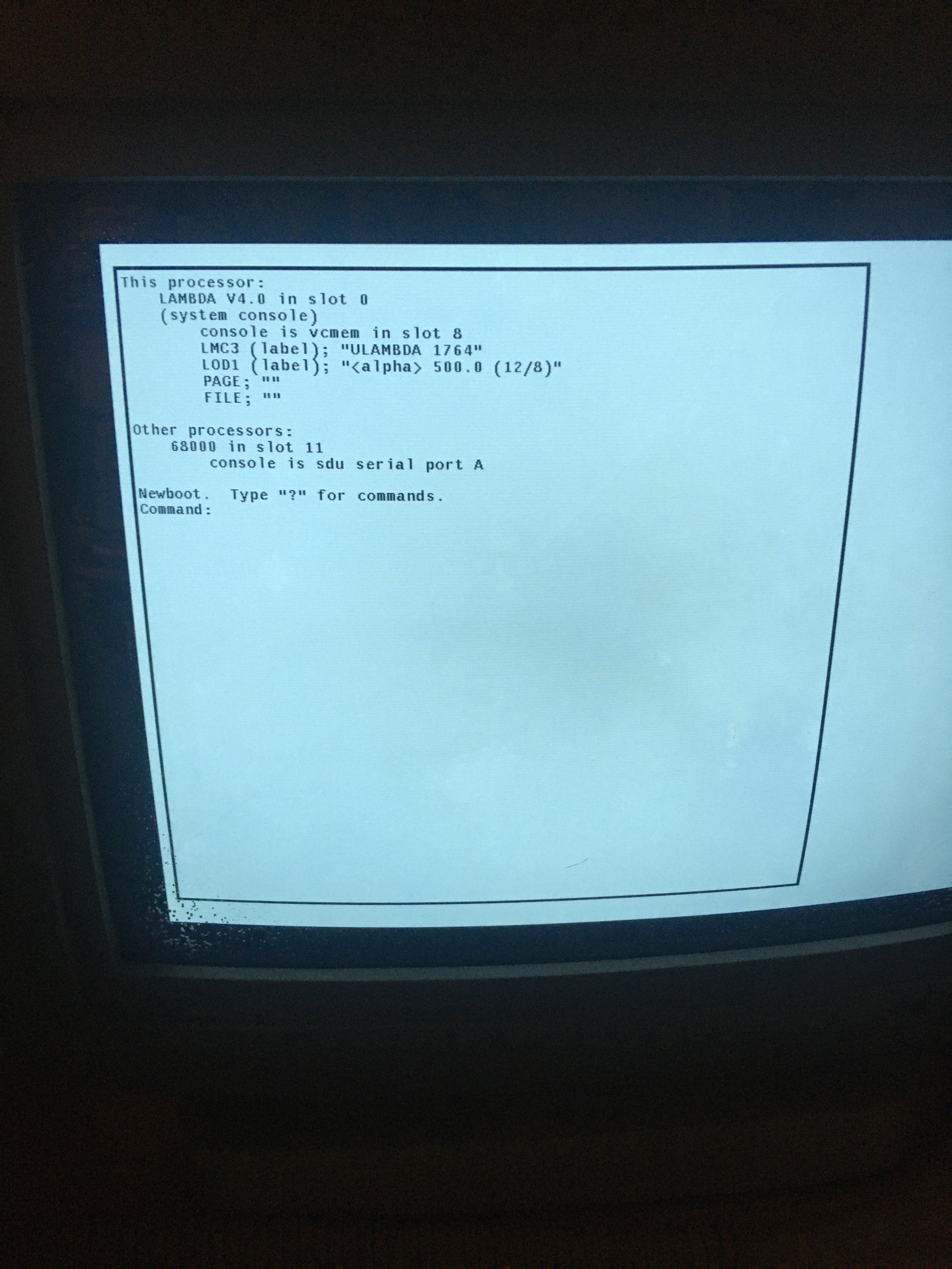
There are three tape files that the install process brings in; you can see them being copied above. The first (“SDU5 3.0 rev 14”) contains a set of tools for the SDU to use, diagnostics and bootstrap programs. The second (“ULAMBDA 1764″) contains a set of microcode files for use by the Lambda processor. The Lambda CPU is microcoded, and the SDU must load the proper microcode into the processor before it can run. The final file (cryptically named ” 500.0 (12/8)” is a load band. (The Symbolics analogue is a “world” file). This is (roughly) a snapshot of a running Lisp system’s virtual memory. At boot time, the load band is copied to the system’s paging partition, and memory-resident portions are paged into the Lambda’s memory and executed to bring the Lisp system to life.


As suspected the tape drive’s throughput was higher during installation than during diagnostic load. But not by much. The above process took about two hours and as you can see it completed without errors, or much fanfare. But it did complete!

Time now for the culmination of the last month’s time and effort: will it actually boot into Lisp? Nervously, I walk over to the LMI’s console, power it on, and issue the newboot command:
The “newboot” herald, inviting me to continue…

Newboot loaded right up and prompted me for a command. To start the system, all you need to do is type boot. And so I did, and away it went, loading boot microcode from disk and executing it, to bring the Lisp system in from the load band. Then the breaker tripped. Yes, I’m still running this all off a standard 15A circuit in my basement, and the addition of the Fujitsu drive has pushed it to its limit. Don’t do this at home, people.

I unplugged the tape drive to reduce the power load a bit, reset the breaker and turned the Lambda on again. Let’s have us another go, shall we?

(I apologize in advance for the poor quality of the videos that follow. One of the side-effects of being stuck at home is that all I have is a cellphone camera…)

(Warning, the above video is long, and also my phone gave out after 3:12. Just watch the first 30 seconds or so and you’ll get the gist of it.)

Long story short: about two minutes after the video above ended, the screen cleared. This normally indicates that Lisp is starting up, and is a good sign. And then… nothing. And more nothing. No disk activity. I gave it another couple of minutes, and then I pinged my friend Daniel Seagraves, the LMI expert. He told me to press “META-CTRL-META-CTRL-LINE” on the keyboard (that’s the META and CTRL keys on both the left and right side of the keyboard, and the LINE key, all held down at once). This returns control to the SDU and to newboot; at this point the “why” command will attempt to provide context detailing what’s going on with the Lambda CPU:


Tell me why, I gotta know why!

Since Daniel knows the system inside and out, he was able to determine exactly where things were going off the rails during Lisp startup. The error being reported indicated that a primitive operator expected an integer as an operand and was getting some other type. This hints at a problem inside the CPU logic, that either ended up loading a bogus operand, or that reported a valid operand as having a bogus type.

Out of superstition, I tried rebooting the system to see if anything changed but it failed identically, with exactly the same trace information from “why.”

In the absence of working diagnostics, schematics, or even detailed hardware information, debugging this problem was going to be an interesting endeavor.

But all was not lost. This is a 2×2 system, after all. There’s a second set of CPU boards in the chassis just waiting to be tested…


This time, after the screen clears (where the video above starts) you can see the “run lights” flashing at the bottom of the screen. (These tiny indicators reflect system and CPU activity while the system is running). Then the status line at the bottom loaded in and I almost fell over from shock. Holy cow, this thing is actually working after all this time!

I have one working Lambda CPU out of the two. I’m hoping that someday soon I can devise a plan for debugging the faulty processor. In particular, I think the missing “double-double” TRAM file opined about in Part 6 of this series has turned up on one of the moldy 9-track tapes I rescued from the Pennsylvania garage — this should hopefully allow me to run the Lambda CPU diagnostics, but it will have to wait until I have a larger disk to play with, as this file resides in a UNIX partition that I don’t currently have space for.

In the meantime since I have a known working set of CPU boards (recall from Part 2 that the Lambda processor consists of four boards), it was a simple matter to isolate the fault to a single board by swapping boards between the sets one at a time. The issue turns out to be somewhere on the CM (“Control Memory”) board in CPU 0.

Meanwhile, not everything is exactly rosy with CPU 1… what’s with the system clock?


System beeps are high-pitched squeaks and the wall clock on the status line counts about 4x faster than it should. Daniel and I are unsure exactly what the cause is at this time, but we narrowed it down to the RG (“ReGisters”) board. In many systems there is a periodic timer, sometimes derived from the AC line frequency (60Hz in the US) that is used to keep time and run the operating system’s process scheduler. The LMI uses something similar, and clearly it is malfunctioning.

Another fairly major issue is the lack of a working mouse. Way back in Part 2 I noted that the RJ11 connector had corroded into a green blob. This still needs repair and as it turns out, getting a working mouse on this system ended up being a journey all its own…

But that’s for my next installment. Until then, keep on keepin’ on!

Lookin’ good, LMI. Lookin’ good.


At Home With Josh Part 7: Putting the “Mass” in “Mass Storage”

Continuing from the conclusion of my last post, I had gotten to the point of testing the LMI’s Interphase SMD 2181 disk controller, but was getting troubling looking diagnostic output:
SDU Monitor version 102 >>/tar/2181 -C Initializing controller 2181: error 3 test 0 Alarm went off - gave up waiting for IO completion 2181: error 3 test 0 Alarm went off - gave up waiting for IO completion 2181: error 10 test 0 no completion (either ok or error) from iopb status iopb: cyl=0 head=0 sector=0 (TRACK 0) 87 11 00 00 00 00 00 00 00 00 00 00 10 00 c5 62 00 40 00 00 00 00 c5 3a
My immediate suspicion was that this was truly indicating a real failure with the controller. The “gave up waiting for IO completion” message was the canary in the coal mine here. The way a controller like this communicates with the host processor (in this case the SDU) is via a block of data in memory that the controller reads, this is the “iopb” (likely short for “I/O Program Block”) mentioned in the output above. The iopb contains the command to the controller, the controller executes that command then returns the status of the operation in the same iopb, and may interrupt the host processor to let it know that it’s done so. (More on interrupts later.)

What the above diagnostic failure appears to be indicating is that the SDU is setting up an initialization command in the iopb and waiting for the 2181 to return a result. And it waits. And it waits. And it waits. And then it gives up after a few milliseconds because the response has taken too long: the 2181 is not replying, indicating a hardware problem.

But the absence of any real documentation or instructions for these diagnostics or the 2181 controller itself left open other possibilities. The biggest one was that I did not at that time have an actual disk hooked up to the controller. The “-C” option to the 2181 diagnostic looked like it was supposed to run in the absence of a disk, but that could be an incorrect assumption on my part. It may well be that the 2181 itself requires a disk to be connected in order to be minimally functional, though based on experience with other controllers this seemed to me to be unlikely. But again: no documentation, anything could be possible.

The lack of a disk was a situation I could rectify. The Lambda’s original disk was a Fujitsu Eagle (model M2351), a monster of a drive storing about 470mb on 10.5″ platters. It drew 600 watts and took up most of the bottom of the cabinet. At the time of this writing I am still trying to hunt one of these drives down. The Eagle used the industry-standard SMD interface, so in theory another SMD drive could be made to work in its stead. And I had just such a drive lying dormant…

If the Eagle is a monster of a drive, its predecessor, the M2284 is Godzilla. This drive stores 160MB on 14″ platters and draws up to 9.5 Amps while getting those platters spinning at 3,000 RPM. The drive itself occupies the same space as the Eagle so it will fit in the bottom of the Lambda. It has an external power supply that won’t, so it’ll be hanging out the back of the cabinet for awhile. It also has a really cool translucent cover, so you can watch the platters spinning and the heads moving: 

The Fujitsu M2284, freshly installed in the Lambda.

The drive is significantly smaller in capacity than the Eagle, but it’s enough to test things out with. It also conveniently has the same geometry as another, later Fujitsu disk that the SDU’s “disksetup” program knows about (the “Micro-169”), which makes setup easy. I’d previously had this drive hooked up to a PDP-11/44 and was working at that time. With any amount of luck, it still is.

Only one thing needed to be modified on the drive to make it compatible with the Lambda — the sector size. As currently configured, the drive is set up to provide 32 sectors per track; the Lambda wants 18 sectors. This sector division is provided by the drive hardware. The physical drive itself provides storage for 20,480 bytes per track. These 20,480 bytes can be divided up into any number of equally sized sectors (up to 128 sectors per track) by setting a bank of DIP switches inside the drive. Different drive controllers or different operating systems might require a different sector size.

The 32 sector configuration was for a controller that wanted 512-byte sectors — but dividing 20,480 by 32 yields 640. Why 640? Each sector requires a small amount of overhead: among other things there are two timing gaps at the beginning and end of each sector, as well as an address that uniquely identifies the sector, and a CRCs at the end of the sector. The address allows the controller to verify that the sector it’s reading is the one it’s expecting to get. The CRC allows the controller to confirm that the data that was read was valid.

What a single sector looks like on the Fujitsu.


The more sectors you have per track, the more data space you lose to this overhead. The Lambda wants 1024-byte sectors, which means we can fit 18 sectors per track. 20,480 divided by 18 is approximately 1138 bytes — 114 bytes are used per sector as overhead. The configuration of the DIP switches is carefully described in the service manual: 

Everyone got that? There will be a quiz later. No calculators allowed.

Following the instructions and doing the math here yields: 20,480 / 18 = 1137.7777…, so we truncate to 1137 and add 1, yielding 1138. Then we subtract 1 again (Fujitsu enjoys wasting my time, apparently) and configure the dip switches to add up to 1137. 1137 in binary is 10 001 110 001 (1024 + 64 + 32 + 16 + 1), so switches SW1-1, SW1-5, SW1-6, SW1-7 are turned on, along with SW2-4. Simple as falling off a log!

With that rigamarole completed, I hooked the cables up, powered the drive up and set to loading the Interphase 2181 diagnostic again:

SDU Monitor version 102
>>/tar/2181 -C
Initializing controller
2181: error 3 test 0 Alarm went off - gave up waiting for IO completion
2181: error 10 test 0 no completion (either ok or error) from iopb status
iopb: cyl=0 head=0 sector=0 (TRACK 0)
87 11 00 00 00 00 00 00 00 00 00 00 10 00 c5 62 00 40 00 00 00 00 c5 3a

Darn. Looks like having a drive present wasn’t going to make this issue go away.

About that time, a local friend of mine had chimed in and let me know he had a 2181 controller in his collection. It had been installed in a Sun-1 workstation at some point in its life, and was a slightly different revision. I figured that if nothing else, comparison in behavior between his and mine might shed a bit of light on my issue so I went over to his house to do a (socially distanced) pickup.

Annoyingly, the revisional differences between his 2181 and mine were fairly substantial:


Two Interphase 2181’s. Can YOU spot the differences?

You can see the commonality between the two controllers, but there are many differences, especially with regard to configuration jumpers — and since (as I have oft repeated) there is no documentation, I have no idea how to configure the newer board to match the old.

So this is a dead end, the revisional differences are just too great. I did attempt to run diagnostics against the new board, but it simply reported a different set of failures — though at least it was clear that the controller was responding.

Well it was well past the time to start actually thinking about the problem rather than hoping for a deus ex machina to swoop in and save the day. I wasn’t going to find another 2181, and documentation wasn’t about to fall out of the sky. As with my earlier SDU debugging expedition, it seemed useful to start poking at the 2181’s processor, in this case an Intel 8085. This is an 8-bit processor, an update of the 8080 with a few enhancements. Like with the SDU’s 8088, looking at power, clock and reset signals was a prudent way to start off.

Unlike with the SDU, all three of these looked fine — power was present, the clock was counting out time, and the processor wasn’t being reset. Well, let’s take a look at the pinout of the 8085 and see what else we might be able to look at:

8085 pinout, courtesy Wikimedia Commons (https://commons.wikimedia.org/wiki/File:Anschlussbelegung_8085.gif)


Oscillation overthruster
The AD0 through AD7 and A15 pins are the multiplexed address/data bus: When the 8085 is addressing memory, AD0-AD7 plus the A8-A15 pins form the 16-bit memory address; when a read or write takes place, AD0-AD7 contain the 8-bits of data being read or written. Looking for activity on these pins is a good way to see if the CPU is actually running — a running CPU will be accessing and addressing memory constantly — and sure enough, looking with an oscilloscope showed pulsing on these pins.

The TRAP, RST7.5, RST6.5, RST5.5, and INTR signals are used to allow external devices to interrupt the 8085’s operation and are typically used to let software running on the CPU know that a hardware event has occurred: a transfer has completed or a button was pushed, for example. When such an interrupt occurs, the CPU jumps to a specific memory location (called an interrupt vector) and begins executing code from it (referred to as an interrupt service routine), then returns to where it was before the interrupt happened. If any of these signals were being triggered erroneously it could cause the software running on the CPU to behave badly.

Probing the RST7.5, 6.5 and 5.5 signals revealed a constant 3.5V signal at RST7.5, a logic “1” — something connected to the 8085 was constantly interrupting it! This would result in the CPU running nothing but the interrupt service routine, over and over again. No wonder the controller was unable to respond to the Lambda’s SDU.

Now the question is: what’s connected to the RST7.5 signal? It could potentially come from anywhere, but the most obvious source to check on this controller is one chip, an Intel 8254 Programmable Interval Timer. As the name suggests, this device can be programmed to provide timing signals — it contains three independent clocks that can be used to provide precise timing for hardware and software events. The outputs of these timers are often connected to interrupt pins on microprocessors, to allow the timers to interrupt running code.

The Intel 8254 Programmable Interrupt Timer
And, as it turns out, pin 17 (OUT 2) of the 8254 is directly connected to pin 7 (RST7.5) of the 8085. OUT 2 is the data output for the third counter, and goes high (logic “1”) when that timer elapses. Based on what I’m seeing on the oscilloscope, this signal is stuck high, likely indicating that the 8254 is faulty. Fortunately it’s socketed, so it’s easy to test that theory. I simply swapped the 8254s between my controller and the one I’m borrowing from my friend and…

Success! Probing RST7.5 on the 8085 now shows a logic “0”, the CPU is no longer constantly being pestered by a broken interval timer and is off and running. The diagnostic LEDs on the board reflect this change in behavior — now only one is lit, instead of both. This may still indicate a fault, but it’s at least a different fault, and that’s always exciting.

Well, the controller is possibly fixed, and I already have a disk hooked up and spinning… let’s go for broke here and see if we can’t format the sucker. The “-tvsFD” flags tell the controller to format and test the drive, doing a one-pass verify after formatting. Here’s a shaky, vertically oriented video (sorry) of the diagnostic in action:


And here’s the log of the output:
SDU Monitor version 102 >> reset >> disksetup What kind of disk do you have? Select one of { eagle cdc-515 t-302 micro-169 cdc-9766 }: micro-169 >> /tar/2181 -tvsFD Initializing controller 2181: status disk area tested is from cyl 0 track 0 to cyl 822 track 9 2181: status format the tracks Doing normal one-pass format ... 2181:at test 0 test reset passed 2181: test 1 test restore passed 2181: test 2 test interrupt passed failedginning of cyl 159 ... at beginning of cyl 0 ... 2181: error 18 test 4 header read shows a seek error iopb: cyl=0 head=0 sector=0 (TRACK 0) 00 00 82 12 00 00 00 00 00 00 00 12 10 00 c5 62 00 40 00 00 00 00 c5 3a 2181: error 18 test 4 header read shows a seek error The 1 new bad tracks are:... bad: track 1591; cyl=159 head=1 ... mapped to track 8229; cyl=822 head=9 There were 1 new bad tracks Number of usable tracks is 8228 (822 cyls). (creating block-10 mini-label) Disk is micro-169 2181: test 5 read random sectors in range passed 2181: status read 500 random sectors 2181: test 6 write random sectors in range passed 2181: status write to 500 random sectors 2181: test 8 muliple sector test passed 2181: test 9 iopb linking test passed 2181: test 10 bus-width test passed 2181: test 0 test reset 0 errors 2181: test 1 test restore 0 errors 2181: test 2 test interrupt 0 errors 2181: test 4 track verify 2 errors 2181: test 5 read random sectors in range 0 errors 2181: test 6 write random sectors in range 0 errors 2181: test 8 muliple sector test 0 errors 2181: test 9 iopb linking test 0 errors 2181: test 10 bus-width test 0 errors >>
And some video of the drive doing its thing during the verification pass:


As the log indicates, one bad track was found. This is normal — there is no such thing as a perfect drive (modern drives, both spinning rust and SSD have embedded controllers that automatically remap bad sectors from a set of spares, providing the illusion of a flawless disk). Drives in the era of this Fujitsu actually came with a long list of defects (the “defect map”) from the factory. A longer verification phase would likely have revealed more bad spots on the disk.

Holy cow. I have a working disk controller. And a working disk. And a working tape drive. Can a running system be far off? Find out next time!